> Another way to make a chip faster is to add special circuits that only do one thing, but do it extremely quickly. Roughly 25 percent of the E5’s circuits are specialized for, among other tasks, compressing video and encrypting data. There are other special circuits on the E5, but Intel can’t talk about those because they’re created for its largest customers, the so-called Super 7: Google, Amazon, Facebook, Microsoft, Baidu, Alibaba, and Tencent. ... If you buy an off-the-shelf Xeon server from Dell or HP, the Xeon inside will contain technology that’s off-limits to you. “We’ll integrate [a cloud customer’s] unique feature into the product, as long as it doesn’t make the die so much bigger that it becomes a cost burden for everyone else,” says Bryant. “When we ship it to Customer A, he’ll see it. Customer B has no idea that feature is there.”
This is something I've never heard of before. Anyone have some insight into this? Is it a relatively recent phenomenon?
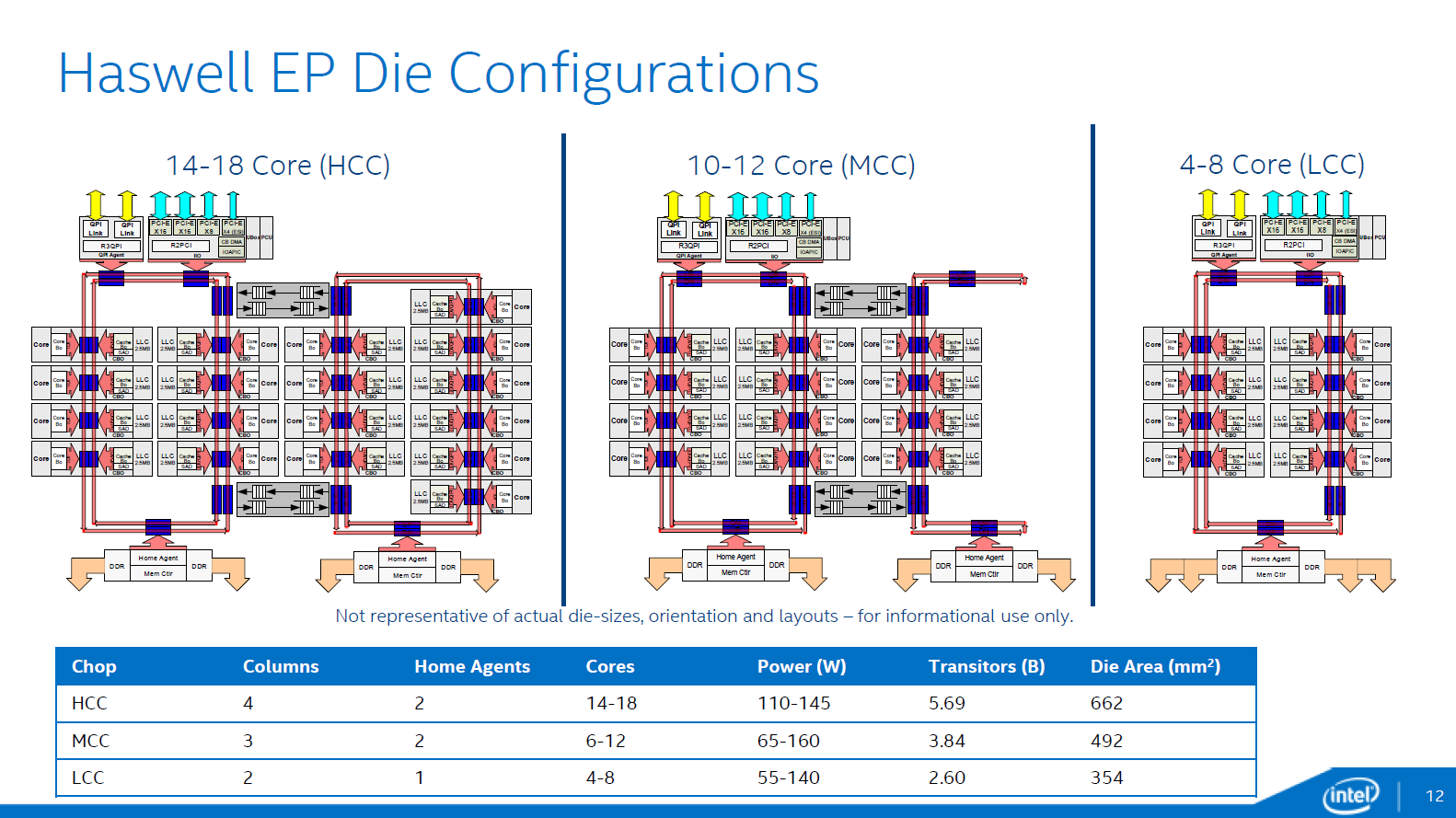
This is also important for the economy of making chips at scale. Since silicon fab is very precise a single wafer can have from dozens to thousands of errors, ranging from failed doping to entire scratches on the surface. Making monolithic all in one chips allows you work around those errors instead of throwing out that part of the wafer.
Say you're making an i7 and half the chips on the wafer have scratches on one or two of the cores. Instead of throwing out half the wafer (doubling the per CPU price) you just disable the damaged cores and sell them as i5s instead.
Yeah sure but there is a tradeoff, making larger (more fully featured) chips also reduces your yield as the chance a chip has a defect is dependant on it's size / surface area.
Dan Luu wrote that Intel's cache allocation tech particularly helped Google, so they could run multiple workloads on one machine without totally trashing the larger caches at every context switch: http://danluu.com/intel-cat/
Someone who follows server chips (maybe AnandTech?) called Xeon D's one of Intel's coolest product lines to come out recently. They're also arguably a smart way for Intel to seal off the lower end of the market against approaches with tons of cheap ARM or AMD cores.
The Zeptobars[1] team and/or Chris Tarnovsky/Travis Goodspeed/Bunnie Huang/et al are probably better equipped for reverse engineering hidden functionality. Anandtech's analyses is great, don't get me wrong, when provided with the proper ISA/datasheets and then giving great critique on what implication feature foo chip bar when it's publically available, but I don't think they're the type of people who take red fuming nitric acid to get the epoxy off chips or are experienced enough in microscopy at the um,nm level to perform such analysis.
Nehalem is the oldest chip I ever saw a floorplan for, and it had a logic block called "misfit" that had special logic requested by a company whose stock ticker you might be able to guess from the block name.
This is not uncommon. Usually a product "family" is all from the same wafer. During packaging and testing either certain pads are not bonded out or certain fuses are blown out (via laser cutting, or as an efuse) to disable certain features that are not available on the lower end version.
In this case Intel is building certain accelerators for some of its customers, and enabling it only for them before shipping it out. I don't think any of these cores contain trade secrets, rather specific functions they've requested which helps accelerate their stack.
They don't try particularly hard to cover that up. It's well-enough known that RDRAND is highly likely to be NSA-backdoored. They could always just shove NSA stuff into the ME anyway (currently there's no reason to believe that they do this, however).
I find it highly unlikely just based on basic economics.
Imagine the potential conversation between Intel and the NSA:
NSA: Please backdoor your RNG for us.
Intel: We're making xx billions of this chip. What happens if someone finds out and we have to recall the chip. Are you paying us the xx billions back then?
NSA: ...
You should look at the Snowden leaks sometime. They had cooperation, including backdoors, in a large number of companies' products and networks. RSA cost them about $30 mil to risk whole market. For carriers, usually around $100 mil or so.
Also, remember that it's easier to do if you disguise it as a coding flaw. It wasn't a backdoor: just one among many flaws accidentally hitting our systems. Wouldn't cost any market share.
Intel has plausible deniability. A backdoor in RDRAND would be some very minor statistical flaw. It could just be something tiny that makes private keys susceptible to some known or unknown attack.
RDRAND is probably microcoded, so they should just be able to patch it out. Since they can't be charged with anything malicious, Intel gets off scot-free.
I don't think he is asking about backdoored functions, but more about specific compute features requested for extremely specific workloads in their datacentres.
Reading this you might get excited thinking wow a secret FPGA hidden in a cpu, in reality they are talking about disabling HT, VT-x, AVX, multiplier change, video encoder/decoder block, AES etc
This is basically the same principle as a GPU - specialized hardware that does one task really well. (In the GPU's case, it's lots of math, very quickly.)
The most common example I can think of is BCH coprocessing, which most modern application processors use for verifying data stored in embedded Flash.
Normally when you think of an ASIC, you think of a single chip custom-designed for a single customer/buyer. You don't think of a single chip with multiple totally different functions and designs consolidated onto it, which get enabled only if they're shipped to the particular customer who requested that particular function. This is like the CPU/GPU core stuff but on steroids - not just 1 or 2 cores disabled to do yield management and price discrimination, but entire processors.
> It’s surprisingly dark, too. For decades, Intel’s cleanrooms have been lit like darkrooms, bathed in a deep, low yellow. “That’s an anachronism,” says Mark Bohr, a small, serious man who has spent his entire 38-year career making chips, and who’s now Intel’s top manufacturing scientist. “Nobody’s had the courage to change it.”
Wait, what? Isn't that UV-free light? Ultraviolet light is used in the mask exposure step, so using normal light in the room would basically remove all of the photoresist before photolithography.
I guess they've automated the process to the point where the wafers are never exposed to light even when moving between steps.
This is true. The wafer carrying "foups" mentioned are actually an acronym for Front Opening Unified Pods, which is what carry the wafers from machine to machine in batches of up to 25 wafers at a time. They are typically UV opaque yellow, or black. The wafers aren't ever actually out in the open in the room at any time.
(As an aside, since the air quality of the room was mentioned...god forbid you ever broke a wafer in the foup. Entire lot in that box is ruined, and cleaning the foup itself and the equipment front ends is a giant PITA)
Source: was engineer at Varian Semiconductor / Applied Materials, who make all those giant tools that Intel and the other fabs use. Intel was definitely one of our largest customers and our most technically demanding.
Oh cool! I was exposed to some tools in a class 100 cleanroom at my research institute. None of them were from Varian though. The lab director always told me that the stuff used in academia is nothing compared to the tools used in large fabs like Intel and TSMC.
By the way, how do tool manufacturers make money? Is it basically sales + maintenance + repairs? Do you have any idea what kind of profit margins they operate on?
Very cool! Money came mainly from sales, but we also offered training courses and had a large services and maintenance division, since the tools did require periodic maintenance. A lot of these tools also have "consumables", just like other large pieces of equipment. Gas sources, graphite liners for beamline components, etc.
As a whole the industry was very cyclical though. We would employ a ton of people in the factories in the years when everyone was moving to new process nodes, but in the years in between there could be lots of manufacturing layoffs / shifts to part time. On the engineering side work was more constant since we would be busy working on the next generation of tools. When I left we were working on the transition from 300mm wafers to 450mm (12 in. to 18 in.)
As far as the profit margins went, I forgot our divisions exact numbers, but AMAT as a whole had roughly ~40% gross profit margins from what I remember. Being on the supplier side of the millions/billion dollar fab builds is a good business :-)
I see, never thought about the demand for tools that way. But that's a pretty damn lucrative business!
I was just looking at the list of top semiconductor equipment manufacturers [1], and it seems that all of them are either American or Japanese companies!
By the way the people at Intel are working with ultra UV, and every material is opaque to them. That is the reason for the use of reflection surfaces instead of lenses for new machines.
Or they've moved so damn far into the UV that their photoresist doesn't even care about the wimpy just-beyond-visual peaks coming out of fluorescent lights.
Everyone's still using 193nm light because it's so painful to go further. It's easier to solve the ridiculous problems involved when etching features a twentieth the size of your wavelength.
They might be referring to the fact that the room might not have photo-resistive materials or the fact that they have not investigated other methods that could allow them to use white light in the room.
"It costs more to make a chip than a plane" - nope, not if you don't build the fabs as Intel does. Of course Bloomberg (or at least many people there) should and does know better.
The point is that if you have a new chip design as a fabless semiconductor start up (like mine), you can get a chip fabbed on a fairly new process node (28nm) for less than $250k for a small quantity run, and go into production for under $5 million through a pure play fab like Global Foundries, TSMC, Samsung, UMC, SMIC, etc.
Oh of course there needs to be fabs, but plenty of them exist. All I was saying is that if you want to make a chip, you don't need to take on Intel's capex.
Then you end up like AMD, with designs that have to be cut back and compromised when a third-party fab doesn't manage to do what they expect on a new process.
There's something to be said for tight integration between fab and design when you're trying to go in to uncharted territory.
If you don't need to be at the edge of process technology, you're completely right of course.
Why do you have to be like AMD - why can't you be like Apple, Qualcomm, NVIDIA, or, well, about any successful/large chip maker other than Intel and Samsung?
Regarding the edge of technology - Intel doesn't beat others to a new node by making both chips and fabs, it would beat others even if it was only building fabs. And it's not like TSMC is that much behind Intel. Grandparent who mentioned 28nm could mention 16nm except that there the masks will costs much more but it's still millions, not billions.
Our next shuttle run is on 16nm... Depending on a bunch of different options, it is "only" ~2-4x the cost of a 28nm run (and should be declining in the next year). Doing a full mask set is still extremely expensive though (~$5-10m range)
   Periodically, the wafer is washed using a form of water
   so pure it isn’t found in nature. It’s so pure it’s
   lethal. If you drank enough of it, it would pull
   essential minerals out of your cells and kill you.
I guess this bit of silliness is our Western version of Korean fan death. It's a commonly-repeated myth that humans need minerals in their water, or that distilled water has meaningful biological effects that "normal" water doesn't. But...
   Bohr’s solution, unveiled in 2007, was to coat parts of
   the transistor with hafnium, a silvery metal not found
   in nature
... somebody had to make that up completely at random.
Who did that, and why did they do it? What goes through a journalist's (or an editor's) head in the process of putting a statement like that in print?
The article is actually pretty interesting... but how much of it am I supposed to believe?
FWIW, they aren't talking about distilled water, they are talking about DI water (deionized), which is different and more reactive / corrosive. Yeah, a sip isn't going kill you, but I wouldn't make a habit of it either.
Sorry, there is absolutely no difference from a physiological point of view.
I've had this argument on here before and am not interested in revisiting it. Suffice it to say that you will be able to find plenty of sources for various old wives' tales along the lines of "Don't drink distilled/DI water, it'll kill you/rot your teeth/give you an itchy rash." None of them will include respected medical texts, legitimate peer-reviewed journals, or even blog posts written by people who remember what their fifth grade Health textbook had to say about the operation of the human kidney.
It's worth objecting to this kind of mythology because some people may assume that the converse implication in the Bloomberg article is also true, and that drinking arbitrarily-large amounts of "normal" water is harmless. The truth is that you will die if you force yourself to drink too much DI or distilled water, and you will die just as quickly if you drink the same amount of tap water.
Fair enough, and I'm not defending the "it will kill you" line, I was just pointing out that they were likely referring to DI water, not distilled as mentioned in the comment, since others may not have heard of / known the difference. Sorry if I didn't make that clear.
I'm not arguing it will kill you, even in more than a sip amounts, and my "don't make a habit of it", was more on the lines of "it's likely not great for your teeth and mouth", since its a bit more reactive, not "OMG THE SPECIAL WATER WILL KILL YOU. ALSO WHAT DID MY 5TH GRADE TEXTBOOK SAY?" Again, sorry if I wasn't clear in my first post!
Quick edit: I don't know if you edited your response or I just missed it the last paragraph (probably the latter) but I whole-heartedly agree on the point of addressing this kind of thing! Totally wasn't trying to argue for accuracy of that statement, just being very nit-picky about it being DI vs distilled...for really no reason what-so-ever, haha.
Why is it so important to make the chips smaller every time? Especially if they're going into servers, where, as the article says, they will almost never be seen by the customers. To go from 2bn transistors to 10bn on something that's already trivially small, why not just make the thing 5 times thicker? Obviously there would be downsides in cost of materials and power consumption, but wouldn't that be offset by avoiding the need for nano-manufacturing advances in every single round? It sounds to me like there's some kind of "manifest destiny" at work here, especially the quote: “Our job is to push that point to the very last minute.” Really?
> Why is it so important to make the chips smaller every time?
Because the amount of power leakage (heat) is proportional to the size of the transistors. So you cannot improve the efficiency of the chip without making the transistors smaller or lowering the frequency.
> Obviously there would be downsides in cost of materials and power consumption,
Huge costs. Data centers aren't only worried about the power consumption of chips, because for every watt that's generated as heat, they have to use >1W to cool that (because cooling systems aren't 100% efficient themselves).
As you may know from other branches of science, the resistance of a conductor rises with heat, meaning that electrons running through the conductor are more likely to hit a vibrating atom and dissipate as heat. This is why so-called "super conductors" are usually super cooled. Very little atom movement = very low chance of an electron hitting a moving atom. Silicon is a semi-conductor, but the principal is the same. If the temperature of the chip rises, so does the heat generated. This is why world-record setting overclocks are done using liquid nitrogen to cool the chip.
To prevent things from getting too toasty, data centers would have to reduce the density of the servers, which means they would need larger buildings and more land to house the same number of servers.
> but wouldn't that be offset by avoiding the need for nano-manufacturing advances in every single round?
> the amount of power leakage (heat) is proportional to the size of the transistors
Small correction: leakage actually increases as transistors shrink. This is why high-k dialectric and fin-fets were such important developments. They pushed back the point at which leakage power overtakes switching power as the dominant source of waste. Even with these technologies, we have to do a lot of design work to reduce leakage. I can't even guess how many power domains are on modern cpus -- certainly dozens if not hundreds. Most of those domains can be switched off to eliminate leakage in those domains altogether.
I'm nearly certain you meant switching power reduces as transistors shrink, which has been true so far. Things are getting weird with these new processes, and a lot of things that we've held as fact are looking less and less reliable.
>Silicon is a semi-conductor, but the principal is the same.
Afaik temperature dependence of materials is a more complicated relation than this. The graph of their coefficient does not even need to be monotone and can change depending on what properties dominate.
E.g. a semiconductor can have NTC because charge concentration increases with the temperature, however when it reaches saturation this effect diminishes and it will behave similar to a regular PTC conductor.
> Huge costs. Data centers aren't only worried about the power consumption of chips, because for every watt that's generated as heat, they have to use >1W to cool that (because cooling systems aren't 100% efficient themselves).
Not at all. A typical cooling system might use 1 watt to move 4 watts of heat outside.
And that's not really how superconductors work. That's how normal conductors work.
Your claim was "Very little atom movement = very low chance of an electron hitting a moving atom." That's something you get in a normal conductor. Low temperature, low resistance. A superconductor has no resistance. This is a very different thing. Completely different effects are taking over to make that happen.
The cost is dependent on the wafer size - bigger is more expensive. Power is dependent on the capacitance of the various switching layers, so smaller features take less power to clock on and off or can go faster. Inductance is dependent on trace length, so shorter traces can be clocked faster or at lower voltages. And that (plus speed-of-light issues) means that smaller chips can both go faster and cost less!
Five wafers stacked on top of each other would take 5 times as much capacity and materials to produce and cost about 5 times as much. The interconnect would be very difficult. Lastly, while you could cool the top wafer, the bottom layers would have to go through a lot of silicon to remove heat. Five times the number of layers on each wafer would also be prohibitively expensive, you don't just cut it thicker, you vapor deposit each layer under a mask and often also need to etch off parts of previous layers or ensure that higher layers are still planar. That gets difficult when you have a few steps of logic layering and some metal layers for interconnect, and would be much more expensive (and hot) with many layers.
This isn't so much of a problem with eg. NAND flash chips which are low power and the address and data pins can just be shared with a couple wafer select wires to separate them, but processors are neither low power nor trivially paralleled.
But assuming you could stack up 5 wafers - and route between them, you get to position transistors in 3d and route them in 3d - which mens wires can be shorter, transistor driving those wires can be smaller and together you could reduce a lot of the wafer area required - maybe by doing 2 layers, you can reduce total wafer area by 50% (but also get much faster low power chip because of the short wires).
The size of the final die is very important to your yield from a single wafer.
Imagine you have a 4in by 4in square. If your chips are 1in^2 you can fit sixteen chips but if your chip is 4in^2, you can only fit four. Now imagine you have a thick scratch going diagonally right down the middle. With the bigger chips, you might lose all four to that single error, wiping out your yield. With the smaller chips however, you'll only lose part of your wafer.
Specialized processors like those made for mainframes or RAD hardened ones can be much bigger since the set up costs will vastly outnumber the fabrication cost anyway. Companies like IBM that aren't in as cost competitive a market as Intel make big chips all of the time.
Until recently, shrinking the process led to some obvious benefits. The chip got faster, cheaper, and more power-efficient. The last part is really the important one and it's why the big datacenter companies kept buying new chips from Intel year after year.
That calculus (so-called Dennard scaling) has now broken down, which is why Intel has abandoned their tick-tock development model in favor of a model that doesn't solely rely on process shrinks in order to achieve better performance.
Or as Intel put it: Our customers expect that they will get a 20 percent increase in performance at the same price that they paid last year. Which is less half as fast as they used to be.
If we make the chip die area bigger the probability of a defect goes up a lot. Similarly with bigger dies, there are fewer dies to a wafer of silicon. All this works out that the die cost is proportional to 4th power of area. So to make money, you want to make the smallest die possible. At the same time you want to add more features which means more transistors. Keeping the die size same means the transistors need to become smaller. Doing that means lots of new improved equipment and research. This also has a cost. So you need to ride the right balance between the two. In most of these companies, the yield rate is one of the most guarded numbers because from that you can estimate costs very easily.
All this feeds into a competitive market between chip manufacturers. If you are a memory manufacturer and can find the right balance that makes the product 5% cheaper to manufacture, they can make a ton of money and gain marketshare. There are a few companies like Apple, Intel that can differentiate on brand name but the rest are commodity products that compete on cost and features.
I think it has to do with distance electricity has to travel. If a chip is physically bigger, it takes longer to move bits inside of it. Sort of similar to why you can't have an L1 cache the same size as main memory.
Just my best guess from a single processor architecture class so definitely not positive that's the answer.
> I think it has to do with distance electricity has to travel.
Correct. The chip has to be small enough that the clock can propagate everywhere within the chip within a single cycle, or problems will occur.
> If a chip is physically bigger, it takes longer to move bits inside of it.
Yes, so either you would need to delay for some cycles to ensure that the information has propagated (which will basically nullify the performance gains from cranking up your clock) or clock parts of the chip differently, but you're pretty much always limited by the slowest part of the chip (which is why every modern chip has a cache, because otherwise it would stall waiting for data).
> The chip has to be small enough that the clock can propagate everywhere within the chip within a single cycle, or problems will occur.
Problems like what? These chips are already chopped up into different clock domains, and it's easy to install some PLLs so that perfectly-synchronized clock signals can blanket a chip even if it's inches across.
Moving data around is also not a big deal. The Xeons in the article already have multi-nanosecond ring busses running around between cores[1]. They don't slow the chip down because the design simply lets long-distance data transfers take multiple cycles. L3 and I/O don't have to be blazingly fast in terms of latency.
> These chips are already chopped up into different clock domains, and it's easy to install some PLLs so that perfectly-synchronized clock signals can blanket a chip even if it's inches across.
Sorry, I didn't explain myself well enough. Of course chips have different clock domains, but these also come at a cost. The more synchronization you need to do between domains, the less die space you have for computationally useful stuff.
> L3 and I/O don't have to be blazingly fast in terms of latency.
I would argue differently, the impact of latency is highly dependent on the type of computation you're doing. If you're doing something with a lot of data (say, encoding video) then you need to be moving data as quickly as possible between the processor and memory. Any additional latency in cache or I/O will cause the performance to suffer.
Ideally, you want the latency of L3 and I/O to be as low as possible.
Ideally you want L3 to be fast, but it's going to be somewhat slow just by the nature of being large. And talking to ram is going to be slow even if the intra-chip pathways are infinitely fast. An extra few percent off-core latency isn't the end of the world if it lets you fit ten times as much computation on the die. L2 and L1 won't be affected.
And encoding video is nearly the platonic ideal of not caring about memory latency. You could easily make memory requests ten thousand cycles before you need the results. You just need throughput.
As others have pointed out, there are several factors. One is that defects in silicon tend to exist in a given areal density. Which means that for a given wafer you'll have, on average, a certain number of defects for a given process, and that in turn translates to the same number of defective chips from that wafer. The more total chips you cram on a wafer then the higher the percentage of non-defective chips you'll get, more or less. Additionally, smaller chips typically mean faster and lower power chips.
Overall these are very very strong factors which push towards shrinking chip size at every opportunity.
> These feats of computer science are often attributed to the rise of the smartphone, but the hard work is being done on thousands of servers. And pretty much all of those servers run on Intel chips.
Considering Intel's recent exit from the smartphone SoC business and concentration on the data center, I have a suspicion why Bloomberg was "given the most extensive tour of the factory since President Obama visited in 2011".
Algolia runs its search service on its own metal for performance. Being off-site [relative to YC] and realtime search not really being critical [relative to YC] might explain some latency.
Anyway, HN's dupe detector isn't all that performent either.
This is something I've never heard of before. Anyone have some insight into this? Is it a relatively recent phenomenon?