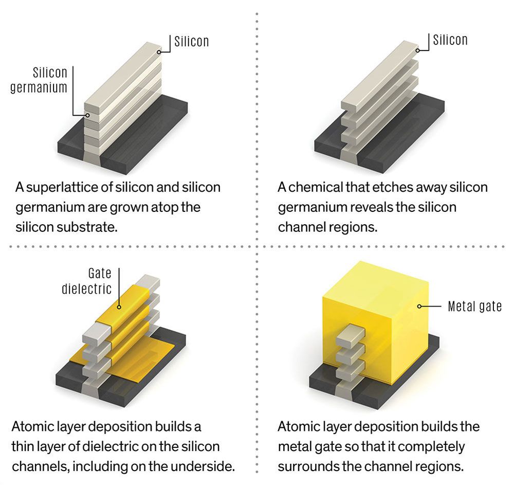
Are there drawings with more detail? I'm unclear where the gate dielectric is and the channel. The silicon is doped differently "inside" the gate to form the channel? That seems hard to fabricate. (I searched around a bit but couldn't find a better diagram.)