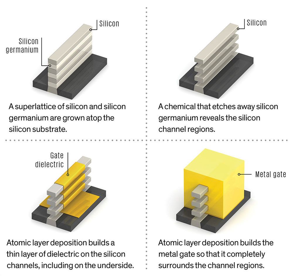
Are there drawings with more detail? I'm unclear where the gate dielectric is and the channel. The silicon is doped differently "inside" the gate to form the channel? That seems hard to fabricate. (I searched around a bit but couldn't find a better diagram.)
Just wanted to point out that 3nm or 2nm are nothing but the marketing terms. The physical channel length will continue to remain at around 10 nm in this decade, irrespective of the device architecture.
See Fig. 1.2 of my PhD thesis: https://etheses.whiterose.ac.uk/22492/1/Novel%20Approaches%2...
Why is that? What’s the point in calling it “3nm” when it’s not?
<rant>
Also, how is that not false advertising then? If I’m told a device is 5nm, and that traditionally meant the gate length, why isn’t it a lie when they’re actually 10nm or whatever? We need to stop calling it “marketing terms” and call it what it is: lies. Just because everyone does it doesn’t make it right.
That is not a great measurement. Transistors can be of different types, each with different value in terms of making products work. Other things matter too: metal, pads, die separation saw cuts, e-fuses, diodes, resistors, and capacitors. Nobody cares about transistors that can't be hooked up to anything.
Well because of tradition. Historically it made sense to define new technology node in terms physical gate length. But now even if that's not viable, they continue to do so for better marketing I guess.
But if we’re not basing it on reality, when does “5nm” become “3nm”? And the fact that it’s just marketing makes comparing across manufacturers (eg. Intel vs. TSMC) impossible.
Short answer is tradition. Historically they were able to stay on Moore's law with each new technology node representing the physical gate length. Currently however, even if they can't continue on that trajectory they still define the next technology node that way.
One thing I've always wondered about when it comes to new process design at smaller scale: how much actual quantum mechanics is actually needed to get the job done?
And ... if the answer is, as I suspect, a lot, what kind of numerical methods and processes are used to design and simulate these tiny quantum mechanical machines?
[EDIT] I mean, when taking a basic QM course, there is a lot of contorsions to try and find analytical solutions to the Schrödinger equation, but as soon as you have three particle interacting with each other, analytical methods run into a wall.
Am I right to think that sub-10nm process design is all done numerically?
Anyone who happens to work on this type of problems care to give pointers?
Depends on what you mean by get the job done. (Rather which job)
If you are doing research into designing advanced transistors with new geometry or new materials (which is what I did my graduate research in), you would be using something like DFT (Density functional theory) for equilibrium analysis and NEGF, Huckel theory etc. for simulating current. These methods only realistically work on ~500-1000 atom systems, beyond which the simulation takes too long to run even on supercomputers (which is what i was using). I think GPUs here would be very useful, but there weren't any tools at the time that were seriously optimized for GPU. The codes I was using were SIESTA/TransSIESTA, Atomistix, QuantumEspresso and others.
For simulating multiple transistors, or transistors with a large geometry (for example 14nm gate length), you would use TCAD simulators that use FEM + measured parameters to simulate the transistors. The equations behind these are traditional semiconductor equations with a bunch of heuristics and curve fitting. The main tool I used was Sentaurus TCAD.
For simulating larger circuits, say a low-noise amplifier or maybe a small DAC, you would use tools like Cadence Virtuoso + the provided PDK from your foundry. The equations here are simpler than the ones used in Sentaurus and they are also calibrated to measurement.
Just as a note, GPU supported code just now seems to be coming on line with like Quantum Espresso GPU version getting an alpha in 2019. I think a large part of that is due to the 64 bit precision making the speed up not as great on GPUs (and to a large extent eliminating the usage of consumer level cards which are popular at the classical molecular dynamics software like GROMACS). Plus Guassian, while having support since Kepler days note that earlier cards didn't have the memory requirements (which also is a huge problem for consumer cards) making adoption slower, because of the added costs.
Thank you for all these pointers, this is really cool.
In particular, I had never heard of DFT ... really intesting and first time I am exposed to what feels like real "hands-on" QM (as opposed to the very stripped down systems one learns about in introductory QM textbooks).
Full disclosure, I don't work on processors but am in a tangentially related field.
However, I don't feel that you need to have an analytical solution to the Schrödinger equation. In fact even in chemistry we don't do analytical solutions instead using fancy basis sets which allow us to do approximations.
Regardless, I don't think even that is particularly necessary, as quantum at that level means you basically have some level of leakage where the electrons can just tunnel through the barrier created by the transistor when off. So if I had to guess most of it is just ways to rectify this leakage so it doesn't effect calculations, probably similar to a form of error correcting.
(This ignores that you may have to do some initial quantum calculations using Density Functional Theorem to get a guess at how much leakage based off the materials you are using, though if I had to guess most of that work was done a while ago.)
Solid State Physics has a bunch of different types of models to try to explain the behavior of electrons in semiconductors and conductors. Most of them are only valid under specific situations and they sometimes give erroneous results unless you apply them carefully. That being said, your absolutely right that the industry uses approximations. They usually use some kind of simulation physics package similar to the ones used by EE engineers when designing circuits.
Hacker news comment sections on articles about semiconductors always seems to be full of people talking authoritatively about things they clearly don't understand. And this is all visible to someone who only majored in computer engineering and got basic training in transistors and logic design who's day job is now in software. I can only imagine the people who actually know transistors cringing in here (and thus avoid commenting).
I worked in an aerospace startup for seven years, and while not an expert I really know my way around some spacey stuff. People speaking authoritatively about that on HN also make me cringe, I rarely intervene because they almost always engage in a discussion about how they are right even when I send references to papers and book chapters. In Reddit it's even worse.
With law and politics I feel there's a similar attitude going around but it's of course more an up for debate topic.
I agree with you (I have been following silicon fabrication news for 20 years already). I cringed when I saw people commenting on, say Intel replacing its CEO, or that RISC-V will replace ARM for design houses in the next few year, when it's clear the commentators haven't taken the time to do even a cursory research.
I don't even want to think of the comments I've seen for my main subject (cybersecurity, exploits, and vulnerabilities). I will never be able to correct all of them.
I think some humility would be nice for all of us. We know what we know and we should be aware of what we don't know. I don't know much about web programming, and I freely admit to it. I certainly don't pretend to have anything insightful to say about them.
I do semiconductor digital physical design for the last 23 years. But almost everything I do is at the standard cell (AND/OR/flip flop) level. I generally don't do anything at the transitor level. I have seen some good comments here in the past.
"Briefly stated, the Gell-Mann Amnesia effect is as follows. You open the newspaper to an article on some subject you know well. In Murray’s case, physics. In mine, show business. You read the article and see the journalist has absolutely no understanding of either the facts or the issues. Often, the article is so wrong it actually presents the story backward—reversing cause and effect. I call these the “wet streets cause rain” stories. Paper’s full of them.
In any case, you read with exasperation or amusement the multiple errors in a story, and then turn the page to national or international affairs, and read as if the rest of the newspaper was somehow more accurate about Palestine than the baloney you just read. You turn the page, and forget what you know.”
It's not just computer engineering. I'm in natural language processing and was in academia and I see a lot of mistakes and misunderstandings in the comments in those topics. Probably the only thing reliable in HN comments is website design.
I tend to disagree; while some comments seem to be clearly wrong, mistakes tend to be pointed out by other commenters, and you can always check bios. It's a bit riskier on stories that don't stay on the front page, I'll grant you that.
And there can be a bit of Dunning-Kruger if you work in a related field too.
It's been a while since node names were actually physical measurements though. For example, at the 3nm node the fin width is 5nm (as noted in the article).
Besides being able to pack more transistors into a given area, a smaller transistor has less gate capacitance (to first order). This means it can switch faster (smaller RC time constant) and less energy is expended in switching. Thus, going from generation to generation, the overall energy expenditure of a chip can be kept within a reasonable range despite adding many more transistors. You also may have heard of a "die shrink", where an existing design gets shrunk to the next technology node, using less power and clocking faster.
Shrinking isn't always a walk in the park though. Some nodes ago subthreshold leakage became a big problem until they figured out how to solve it.
Smaller distance -> lower resistance -> less heat -> higher clocks/more stuff per clock allowed with same amount of heat produced -> higher performance.
Smaller dimensions means you can set a smaller length for the wire.
As you can see on the diagram on this article, there is a large push into increasing the height of the transistors. That has being going on for more than a decade.
About the width, a finer process means you can keep the width of the most critical transistors the same, but can also trade it off into less width (and performance) where it is less important.
So, overall, smaller dimensions leads to lower resistances. You can trade some of the gain for density, but you'll always get some lower resistance.
None of these reasons are as important as transistor count / mm^2. If you can shrink die size in half, you can effectively reduce its cost by half as well. Processing wafers through 400 steps in the fab and its capacity is limited by how many useful chips you can build on a given 300mm wafer.
Exactly, the smaller your chip is the more you can fit on a silicon wafer.
If your chip is too large it can even make it practically impossible to manufacture at scale due to the increased chance of defects as your chip size increases.
It's crazy to think about if you've never thought about this, but the speed of light is a bottleneck for processors. When we get smaller devices, there's literally less distance that needs to be traversed, so more can be done!
An electrical signal travels close to the speed of light (not the electrons). Even when of course no light travels inside the copper.
If something oscillates at 1 GHz, 15 cm down the wire the phase is opposite. To me it's perfectly correct to say that speed of light affects the design a lot and in many places probably is a bottleneck.
And the "electric signal" is an electromagnetic wave- also known as light. Nowhere did they imply the speed of light in a vacuum, the speed of light in copper is an equally valid interpretation.
More charitably, charge carriers do move much more slowly than the electric field they transmit[0], and while you’re correct that the time-varying electric field in a processor is not light (nor even a radio wave), if the chips were much larger or much higher frequency the chips and buses would risk becoming antennas and having all the problems that would bring — 5 Ghz ~= 6cm wavelength [1] ~= 3cm half-wave dipole.
The numbers roughly correspond to the width of wires in the circuits, but the number of circuits you can fit per unit area depends on the square of that number so going from 7nm to 5nm roughly doubles density. The first microprocessor[1] was around 10,000nm so we're approaching 5,000x thinner wires or almost 25 million times more circuits (the latest Apple M1[2] is at 5nm have about 8,000,000x as many transistors as the 4004).
Smaller distance to travel so signals get from one gate to another quicker which will enable a higher clock speed.
Smaller devices use less power so less heat and longer battery life.
Smaller devices mean a smaller chip which is cheaper (although mask costs will be more expensive) or use the extra area for more features like more cache or another processor core.
With a Fixed Yield, and an exact 100% increase in Transistor Density that translate to 50% smaller Die Size.
On a Wafer, that would equate to Double the amount Die you have. All of a sudden your profits increase dramatically.
5nm also have a better power curve so within the same clock speed you have lower energy usage. Hence you can push for higher performance if needed.
The first point of Uni Economics is important for the industry. If you have high enough volume, say hundreds Million of chips per year then it make sense to move to the next node for cost saving. If you have small volume or low margin chip then the Design Cost, which is the most expensive part of chip making, would not work to your benefits.
And it also depends on Wafer price, If 5nm is Double the Price of 7nm then in the above example your unit cost would be exactly the same.
The second point is important for CPUs, and other things that are increasingly computational expensive like WiFi 6 and 5G Modem. You want your Smartphone to last longer on battery so they work better on an energy efficient node.
So basically it is a Cost / Performance trade offs.
Smaller means closer together. Closer together means less time for a signal to move from one to another. Less time means higher clock speeds.
If you CPU is 100mm across, the speed of light limits it to 3GHz because that's how many times you can cross the cpu travelling at c. At 10mm you get 30GHz.
I don't really know enough to refute it, but this seems deeply and bizarrely wrong. It doesn't account for transistor count or density just the size of the entire chip? With pipelining I don't think a signal has to travel across the entire chip every cycle. It also doesn't really address the question above, since single core CPU speeds haven't increased in 15 years even though transistors have kept getting smaller and closer together.
Seems like an intriguing napkin math limit/simplification though, I'd be interested if anyone could elaborate on if there's any substance to it.
The speed of EM signal in copper is roughly 60% of the speed of light. You also have to account for timing jitter and wait until you are sure that everybody has the signal to prevent going out of sync.
This means that reliable distance from a single clock is just a fraction of what the speed of signal theoretically allows.
Clock distribution networks use local clocks to buffer and amplify the global clock but they take a significant amount of chip area and make the chip larger. Clock distribution circuitry draws a significant amount of power. It can be 30-40% of the power usage. You want to use them as little as possible.
It is not wrong, it is rather correct. Speed of propagation in semiconductor materials is at most a third of speed of light in vacuum. So the distance travelled is rather limited for a signal. Also, a signal might have to traverse a few transistors or gates, so frequency in the 3GHz range does really limit processor sizes to the order of millimeters. You already said how to get around it: Pipelines, that limits the area a signal has to propagate. Also, one has to take care to make signals arrive early enough in the longest possible signal path as well as to distribute the clock in a way for it to arrive at aligned times everywhere, so you need a clock distribution net with known delays, etc. Chip timing is black art.
When designing chips or doing layout for FPGA designs, we do something called timing analysis to find out if signals get to where they should do such that the chip is stable ("meets timing").
There is a lot more to it than just distance. The transistors have speeds, to start with.
That and just because this size gives a bound on how quickly you can do things, the transistor count is also increasing, so the actual clock doesn't increase all that much.
> If you CPU is 100mm across, the speed of light limits it to 3GHz because that's how many times you can cross the cpu travelling at c. At 10mm you get 30GHz.
100mm across is 10cm, 0.1m, 4 inches. That’s palm-sized CPU - far from any modern silicon.
Rather than the change in transistor design, I think the bigger news is the switch from silicon with dopants to silicon with germanium and dopants. The drop in threshold voltage from ~0.7v to ~0.3v might be one of the last levers left in extracting even more performance; at the cost of making semi production and equipment even more hazardous.
What do you mean "silicon with germanium and dopants"? Implanting germanium as a dopant is already done at much larger geometries than 2/3nm. It's also not any more hazardous than implanting any other ion.
I think parent might have confused Germanium with Cadmium? I am no chemist. It could also require other more toxic substances to control reactions or act a carrier. The whole area around Sunnyvale is littered with toxic waste dumps from semiconductor manufacturing. [1] From [2], it says, "Some reactive intermediate compounds of germanium are poisonous", when then references [3] but I can't find the specific citation. I think Germanium is getting lumped in with other toxic chemicals used in semiconductor manufacturing like gallium arsenide, cadmium, etc.
Per transistor maybe, but the leakage goes down less than the amount of transistors you can pack per area, so in effect, per die/chip your leakage increases. Heat as well, but it’s the other side of the same coin.
From what I can gather looking at the images and such, the device is one gate with 3 or more isolated channels, each with separate source/drains. Are these processes constrained such that all the sources/drains have to be linked together later? Or can they be used independently, allowing the designer to construct 3 or more transistors with a shared gate?
I think what the world needs more right now is more foundries and not smaller manufacturing processes. The global chip shortage totally sucks and it's because there's so few players and all the innovation is focused on stuff like this instead of figuring out ways to produce ICs faster and cheaper.
Note that "MBCFET" is Samsung's name for their "nanosheet" FET.
And the Anandtech article it comes from: https://www.anandtech.com/show/16041/where-are-my-gaafets-ts...